 Products Home / Custom Solutions & Manufacturing Capabilities / Optics Capabilities / Pattern-Transfer Nanomanufacturing (PTNM)
Pattern-Transfer Nanomanufacturing (PTNM)

- Fast, Efficient Alternative to Traditional Nanolithography Techniques
- Fabricate Patterned Optics such as Gratings or Create Arbitrary 2D Patterns
<25 nm
Write Master
Create Photolithographic Mask
Transfer Pattern
Etch Substrate

Please Wait
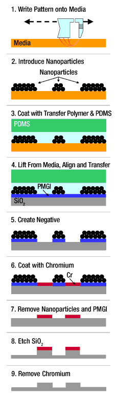
Figure 1.1 Example PTNM Process
PTNM for Nanolithography

Jason Williamson
Director of Business Development
Thorlabs Spectral Works
Questions?
Custom or OEM Applications?

At the beginning of May 2019, Thorlabs welcomed Cirtemo and their Pattern-Transfer Nanomanufacturing (PTNM) technology. This team joins us as Thorlabs Spectral Works, devising innovative solutions to nanolithography.

Click to Enlarge
Figure 1.2 Arbitrary 2D PTNM
Capabilities
- Patterns on PVA, PMMA, PDMS, Fused Silica, and Sapphire
- Surface Type: Curved Lenses, Wafers, Mirrors, and Fiber End Faces
- Feature Size:
- <25 nm Feature Resolution
- 300 nm Between Features
- Up to 1.5 µm Feature Depth
- Transmission or Reflection Gratings:
- Blazed Triangle and Binary Profiles
- 200 nm to 1600 nm Wavelengths
- >90% Diffraction Efficiency (Wavelength Dependent)
Applications
- Gratings: Plane, Curve, Variable, or Mosaic
- Resolution Test Targets and Reticles
- Fresnel Zone Plates
Pattern-transfer nanomanufacturing (PTNM) technology provides a low-cost, efficient alternative to traditional nanolithography techniques. PTNM builds on the 50+ years of research and development in hard disk drive technology, creating photolithographic masks with features on the scale of tens of nanometers. The process is ideal for producing custom diffractive optical elements for use in the UV to IR spectral range. The written patterns can be applied to numerous substrate materials such as polymers, silicon wafers, fused silica, and optical fiber tips.
The key to PTNM is the magnetic recording read/write head, which is brought into contact with magnetic recording media as shown by Step 1 of the sample procedure in Figure 1.1. The operating principle is identical to that of hard disk drive heads, allowing a user-defined 2D template to be created by controlling magnetic transitions with high spatial resolution. Similarly, any template created will be stable for years and can be erased or rewritten.
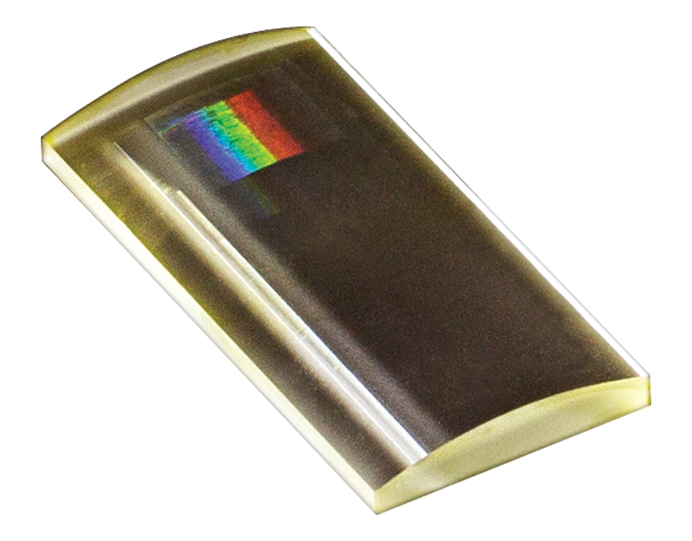
After introducing the 2D template into a magnetic nanoparticle suspension, the nanoparticles will self-assemble on the magnetic transitions, as shown in Figure 1.3. This master pattern may then be transferred and etched with subsequent procedures (Figure 1.1, Steps 3 to 9), creating products such as the grating on the cylindrical lens or fresnel zone plate shown in Figure 1.5. Alternatively, the master pattern could be used as a custom life-science substrate if the magnetic particles are functionalized. The manufacturing flexibility offered by PTNM can open up new possibilities for life-science and photonics applications.
Thorlabs Spectral Works also designs, models, and builds multivariate optical elements for analyte detection with high specificity and efficiency. Click here to learn more.


| Posted Comments: | |
| No Comments Posted |