 Products Home
Surface-Enhanced Raman Spectroscopy (SERS) Substrates
- Gold-Coated Textured Quartz Substrates
- Plasmonic Nanostructures Enhance Raman Scattering Signal
- Parts Per Billion Sensitivity
- Optimized for 785 nm Laser Excitation
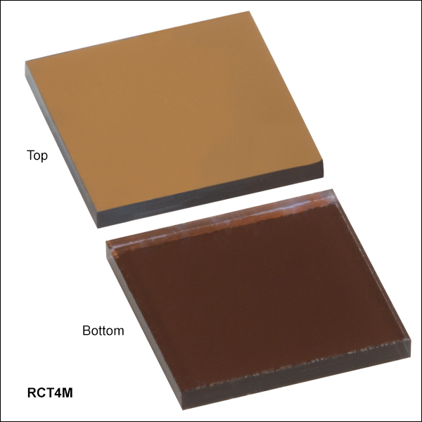
RCT4M
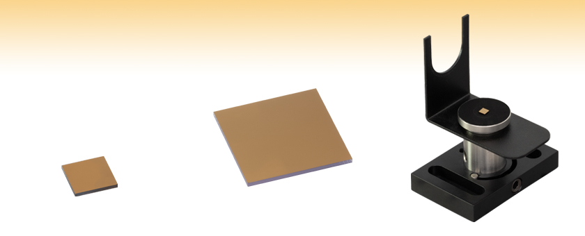
4.3 mm x 4.3 mm Active Area
Application Idea
The RCT4M Gold-Coated SERS Substrate can be mounted to the RSBR1(/M) sample stage. Please see the Overview tab for more information.
RCT10M
9.5 mm x 9.5 mm Active Area


Please Wait
 Click to Enlarge
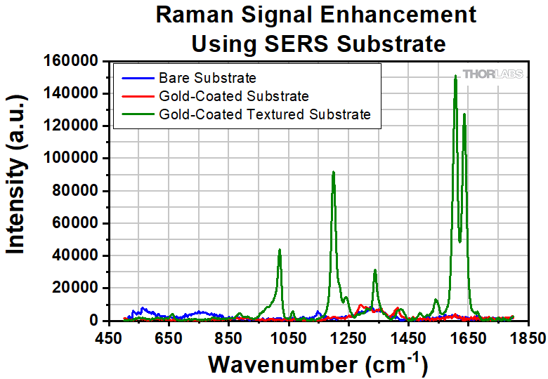
Figure 1.1 This graph shows the effects of SERS on the Raman signal of 1 mM 1,2-di(4-pyridyl)ethylene. All samples were prepared using the same immersion method. Data was collected using the RSB1 Raman kit with 785 nm laser excitation and a 5 second integration time. The laser spot size was 1.5 mm2 and the power was set to 10 mW.
 Click to Enlarge
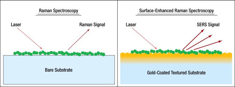
Figure 1.2 An illustration to show the difference between Raman spectroscopy and Surface-Enhanced Raman Spectroscopy. In SERS, incident laser later creates an electric field that increases the probability of Raman scattering, thereby enhancing the measured Raman signal.
Got Questions?
Our engineers and expertise are here for you!

Jason Williamson
Director of Business Development
Thorlabs Spectral Works
If you are not sure whether our catalog SERS substrates meet your needs, we invite you to contact us to discuss your specific application, including custom or OEM requirements you may have.
Just press the button, and we'll get back to you within the next business day.

Features
- Gold-Coated Textured Fused Quartz Substrates for Surface-Enhanced Raman Spectroscopy (SERS)
- Plasmonic Nanostructures Enable Parts Per Billion Sensitivity*
- Compatible with Thorlabs' Modular Raman Kit and Portable Raman Spectrometer
- Square Substrates with 4.5 mm or 10.0 mm Edge Lengths and >90% Active Area
- Single-Use Substrates with 6 Month Lifetime Outside of Vacuum
- Volume Quantities and/or Custom Sizes Available
Applications
- Detection of Fingerprint Signals from Molecules
- Quantitative Analysis of Chemical Mixtures
- Identification of Illegal or Dangerous Substances
- Quality Inspection (Pharmaceuticals, Food, etc.)
- Monitoring Chemical Processes at Production Sites
Thorlabs' Surface-Enhanced Raman Spectroscopy (SERS) Substrates are designed for SERS, a subset of Raman spectroscopy that can enhance the Raman scattering of a sample by orders of magnitude. Each SERS substrate is made from a textured fused quartz substrate with gold deposited on the surface, creating plasmonic nanostructures that enable sensitivity down to parts per billion.* More than 90% of each chip's top surface is SERS active.
Raman scattering is a rather rare event and occurs for only about 1 in 1 million exciting photons. Therefore, it is typically necessary to excite the sample with a high-power light source. SERS is a technique that can enhance the Raman scattering of a sample by using a metal surface as a sample substrate. There are two primary mechanisms that cause this enhancement. The first is an electric field enhancement, which is created by the excitation of localized surface plasmons. When molecules under interrogation are within the presence of this electric field, the probability of Raman scattering increases greatly. The second mechanism is a chemical enhancement due to inter- and intra- molecular charge transfer between the metal and molecule of interest. This makes SERS a non-destructive, highly sensitive technique that can be used to measure extremely low sample concentrations with significantly lower incident laser power in comparison to a standard Raman measurement.
Usage, Handling, and Care
Samples can be prepared on the SERS substrates using a drop-cast method. Simply place 2 to 10 µl of aqueous solution onto the gold side of the substrates using a micropipette (note that the top, active surface is gold while the bottom surface is brown). Alternatively, if sample volume is abundant, an immersion method can be used by placing the substrates in a bath of solution, incubating for 10 minutes, and rinsing with water or ethanol. Let the sample dry completely before placing in the Raman spectrometer. Please note that substrates are single use and we do not recommend washing.
 Click for Details
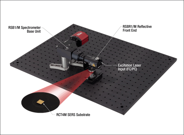
Figure 1.3 These SERS substrates can used with the RSB1(/M) spectrometer. Here, the RCT4M substrate is shown mounted on the RSBR1/M reflective front end sample stage with the active side facing up.
Thorlabs recommends using gloves and tweezers when handling these SERS substrates. To avoid damaging the plasmonic nanostructures, the active gold-coated surface of the substrates should not be touched directly. If needed, we recommend removing dust from the surface using clean, dry compressed air, as detailed in the Blowing Off the Surface of an Optic section in our Optics Handling and Care Tutorial.
The SERS substrates are packaged inside a vacuum sealed bag. For best performance, it is recommended to use the SERS substrates within 6 months when outside of vacuum.
Mounting
To avoid damaging the plasmonic nanostructures and contaminating instrumentation, ensure the active surface of the SERS substrates does not make direct contact with the mounting surface. When using with our Modular Raman Spectroscopy Kit equipped with the reflective front end, place a substrate on the sample stage with the active side facing up (see Figure 1.3). The laser beam can then be aligned to the center of the substrate. When mounting a substrate to our Portable Raman Spectrometer, it is important to make sure the active surface does not come in direct contact with the sample window. The RCT4M SERS substrate is compatible with the CDH45 adapter for square optics. For more information on the recommended mounting procedure or to discuss mounting options with the RASP spectrometer, please contact Tech Support.
*Sensitivity is dependent on the experimental conditions, including the analyte, incident laser power, and integration time.
 Click to Enlarge
Click Here for Raw Data
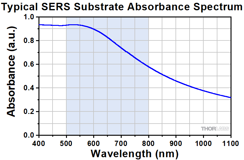
Absorbance spectrum of a typical SERS Substrate. The substrate is optimized for use with 785 nm excitation; however, the broadband absorbance enables its use with other excitation wavelengths (depicted by the blue highlighted region).
Click to EnlargeThis graph shows the effects of SERS on the Raman signal of 1 mM 1,2-di(4-pyridyl)ethylene. All samples were prepared using the same immersion method. Data was collected using the RSB1 Raman kit with 785 nm laser excitation and a 5 second integration time. The laser spot size was 1.5 mm2 and the power was set to 10 mW.

Click to Enlarge
Figure 3.1 Energy Levels of Various Radiation Types
Raman Spectroscopy
Raman Spectroscopy is a well-established technique for the characterization of chemical substances in solid, powder, liquid, or gas forms. It is based on the detection and analysis of Raman scattered light emitted from a sample upon exposure to monochromatic light.
Raman Scattering
Atoms in a molecule are held together by chemical bonds. Depending on the number of atoms and the geometry of the bonds, there are different ways molecules can vibrate. Each unique mode of vibration can be excited only with a certain, well defined amount of energy. When an exciting photon is absorbed by the molecule, it may excite a vibrational mode or absorb energy from an existing vibrational mode before being re-emitted. The loss or gain of energy due to this interaction with a vibrational mode means the photon is inelastically scattered, and this interaction between the light and the material is called the Raman effect. The resulting shift in energy and wavelength of the scattered photon due to this inelastic scattering (Raman scattering) is called the Raman shift. Raman spectroscopy measures this Raman shift.
Raman scattering is a rather rare event and occurs for only about 1 in 1 million exciting photons. It is, therefore, critical to excite the sample with a high-power light source and to collect as much Raman-scattered light as possible for analysis. To generate sufficient Raman scattering, the sample is typically exposed to high-intensity monochromatic laser light.
Because excitation of a whole set of vibrational states of a sample with a defined amount of energy (the exciting laser light) results in material-specific Raman scattering, a measured Raman spectrum may be considered a chemical fingerprint of the substance. The vibrations detected by Raman spectroscopy may differ from those modulating the molecular dipoles, which are observable by IR spectroscopy, and make it a valuable source for material analysis and complementary to other types of vibrational spectroscopy.
Energy Shift Due to Inelastic Scattering
Raman spectroscopy analyzes the shift in energy due to inelastic scattering caused by the Raman effect. The wavelength of the inelastically scattered photon is related to the excitation wavelength through energy Equation 1 describing the Raman scattering event:
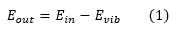
where Evib is the vibrational energy of the molecule affected by the exciting photon, Eout is the energy of the scattered photon, and Ein is the energy of the exciting photon.
The photon's energy and frequency are related via the Planck-Einstein relation:

with h = 6.6260715 x 10⁻³⁴ J⋅s, fin is the incoming photon frequency in Hertz. The analogous relation holds for the scattered photon (Eout = hfout).
Using Equations 1 and 2, as well as λ = c/f where c is the speed of light, the Raman shift of a molecular vibration can be characterized with knowledge of the precise wavelength of the excitation wavelength λin based on Equation 3:

Describing Raman scattering in wavelength space is a disadvantage, as it depends on the precise excitation wavelength. However, it is fixed in the Raman-shift scale, or wavenumber scale, in units of cm-1. Therefore, in order to compare Raman spectra of a substance between different experimental setups, Raman spectra are represented as 2D plots of measured relative intensity (Y-axis) in Raman shift of the inelastic scattered light in wavenumbers (cm-1, X-axis). This unit is, in contrast to nanometers, a scale proportional to energy.
| Posted Comments: | |
| No Comments Posted |
 Substrates")
 Zoom
Zoom| Key Specifications | ||
|---|---|---|
| RCT4M | RCT10M | |
| SERS Active Material | Gold | |
| Active Area |
4.3 mm x 4.3 mm | 9.5 mm x 9.5 mm |
| Laser Wavelength (Recommended) | 785 nm | |
| Minimum Power Densitya (Recommended) |
0.1 W/cm2 | |
| Lifetimeb (Recommended) | <6 Months | |
| Physical Dimensions (L x W) |
4.5 mm x 4.5 mm (0.18" x 0.18") |
10.0 mm x 10.0 mm (0.39" x 0.39") |
| Substrate Thickness | 0.500 mm (0.0197") | |
- Gold-Coated Textured Fused Quartz Substrates
- Optimized for 785 nm Laser Excitation
- Compatible with Thorlabs' Modular Raman Spectroscopy Kit and Portable Raman Spectrometer
- Square Substrates with 4.5 mm or 10.0 mm Edge Lengths and >90% Active Area
- Available in 5 Packs
The RCT4M and RCT10M Surface-Enhanced Raman Spectroscopy Substrates are designed for use in SERS to enhance Raman scattered signal by orders of magnitude. The gold-coated textured quartz substrates enable sensitivity down to parts per billion,* allowing for the measurement of low sample concentrations with significantly lower laser powers in comparison to standard Raman spectroscopy. More than 90% of each chip's top surface is SERS active.
These SERS substrates are optimized for 785 nm laser excitation and are compatible with Thorlabs' Modular Raman Spectroscopy Kit and Portable Raman Spectrometer. Aqueous samples can be placed directly on the top gold-coated side of a substrate. When mounting to a Raman system, the excitation laser should be incident on this surface. The RCT4M SERS substrate is compatible with the CDH45 adapter for square optics. Please note that the SERS substrates are single-use and washing is not recommended.
The SERS substrates are packaged inside a vacuum sealed bag. For best performance, it is recommended to use the substrates within 6 months when outside of vacuum.
*Sensitivity is dependent on the experimental conditions, including the analyte, incident laser power, and integration time.